- 您现在的位置:买卖IC网 > Sheet目录1998 > ICS84314AY-02LFT (IDT, Integrated Device Technology Inc)IC SYNTHESIZER 700MHZ 32-LQFP
ICS84314-02
700MHZ, CRYSTAL-TO-3.3V/2.5V LVPECL FREQUENCY SYNTHESIZER W/FANOUT BUFFER
IDT / ICS 3.3V/2.5V LVPECL FREQUENCY SYNTHESIZER
3
ICS84314AY-02 REV. A MARCH 24, 2009
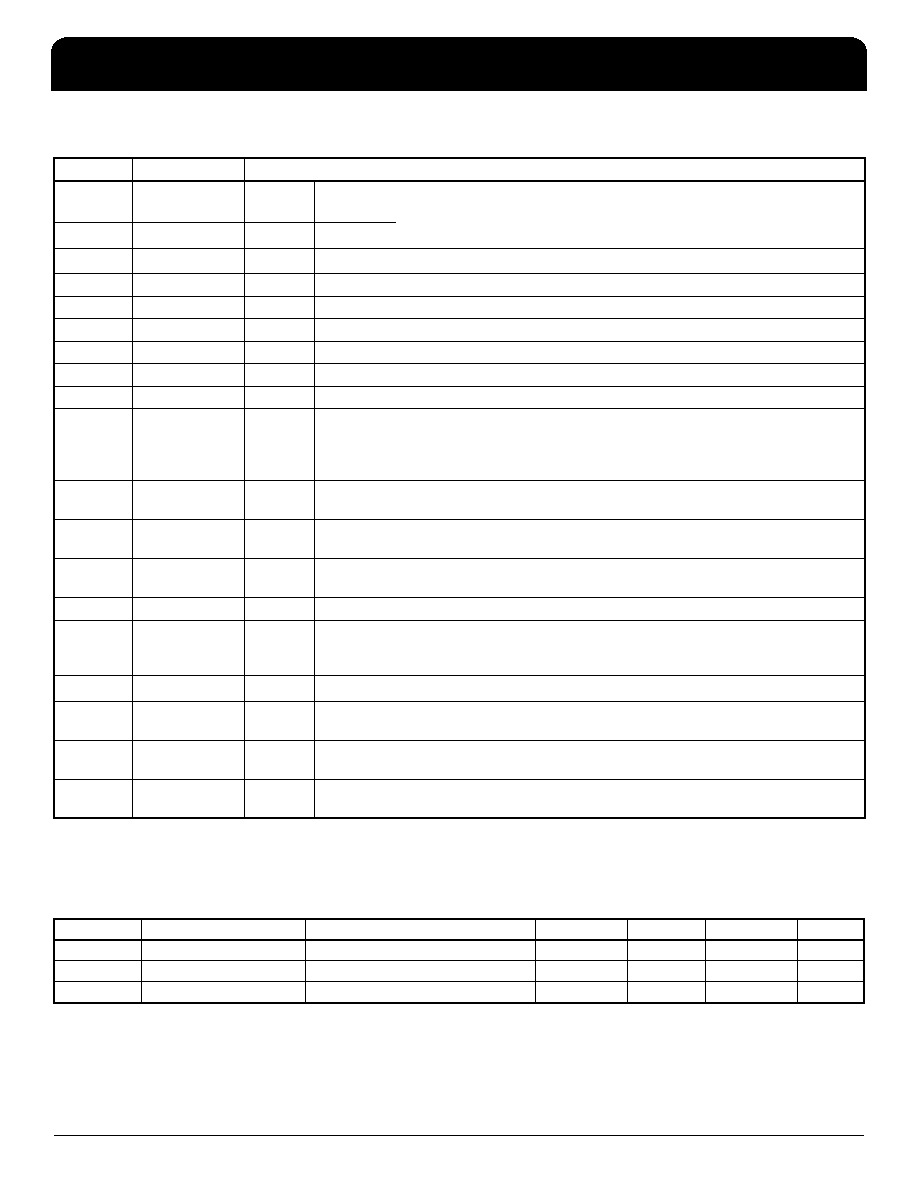
Table 1. Pin Descriptions
NOTE: Pullup and Pulldown refer to internal input resistors. See Table 2, Pin Characteristics, for typical values.
Table 2. Pin Characteristics
Number
Name
Type
Description
1, 2, 5,
29, 30, 31
M4, M5, M8
M0, M1, M2
Input
Pulldown
M divider inputs. Data latched on LOW-to-HIGH transition of nP_LOAD input.
LVCMOS / LVTTL interface levels.
3, 4, 32
M6, M7, M3
Input
Pullup
6VEE
Power
Negative supply pin.
7VCC
Power
Core supply pin.
8, 17
VCCO
Power
Output supply pins.
9, 10
Q0, nQ0
Output
Differential clock outputs for the synthesizer. LVPECL interface levels.
11, 12
Q1, nQ1
Output
Differential clock outputs for the synthesizer. LVPECL interface levels.
13, 14
Q2, nQ2
Output
Differential clock outputs for the synthesizer. LVPECL interface levels.
15, 16
Q3, nQ3
Output
Differential clock outputs for the synthesizer. LVPECL interface levels.
18
MR
Input
Pulldown
Active High Master Reset. When logic HIGH, the internal dividers are reset
causing the true outputs Qx to go low and the inverted outputs nQx to go high.
When logic LOW, the internal dividers and the outputs are enabled. Assertion
of MR does not affect loaded M values. LVCMOS / LVTTL interface levels.
19
S_CLOCK
Input
Pulldown
Clocks in serial data present at S_DATA input into the shift register on the
rising edge of S_CLOCK. LVCMOS / LVTTL interface levels.
20
S_DATA
Input
Pulldown
Shift register serial input. Data sampled on the rising edge
of S_CLOCK. LVCMOS / LVTTL interface levels.
21
S_LOAD
Input
Pulldown
Controls transition of data from shift register into the dividers.
LVCMOS / LVTTL interface levels.
22
VCCA
Power
Analog supply pin.
23
XTAL_SEL
Input
Pullup
Selects between the crystal oscillator or test clock as the PLL reference
source. Selects XTAL inputs when HIGH. Selects TEST_CLK when LOW.
LVCMOS / LVTTL interface levels. See Table 3F.
24
TEST_CLK
Input
Pulldown
Single-ended test clock input. LVCMOS / LVTTL interface levels.
25,
26
XTAL_IN,
XTAL_OUT
Input
Crystal oscillator interface. XTAL_IN is an oscillator input, XTAL_OUT is an
oscillator output.
27
nP_LOAD
Input
Pulldown
Parallel load input. Determines when data present at M8:M0 is loaded into the
M divider. LVCMOS / LVTTL interface levels.
28
VCO_SEL
Input
Pullup
Determines whether synthesizer is in PLL or bypass mode.
LVCMOS / LVTTL interface levels. See Table 3G.
Symbol
Parameter
Test Conditions
Minimum
Typical
Maximum
Units
CIN
Input Capacitance
4
pF
RPULLUP
Input Pullup Resistor
51
k
RPULLDOWN
Input Pulldown Resistor
51
k
发布紧急采购,3分钟左右您将得到回复。
相关PDF资料
ICS843156AKILF
IC CLK GENERATOR 32VFQFP
ICS843156AKLF
IC CLK GENERATOR 32VFQFP
ICS843202AYILF
IC SYNTHESIZER 680MHZ 32-LQFP
ICS843204AGILF
IC SYNTHESIZER LVPECL 48-TSSOP
ICS84320AY-01LN
IC SYNTHESIZER GP LVPECL 32-LQFP
ICS84320AYI-01LF
IC FREQ SYNTHESIZER 32TQFP
ICS843251AG-04LF
IC CLK GENERATOR LVPECL 8-TSSOP
ICS843251AGI-14LF
IC CLK GEN ETHERNET 25MHZ 8TSSOP
相关代理商/技术参数
ICS84314AY-02T
制造商:ICS 制造商全称:ICS 功能描述:700MHZ, CRYSTAL-TO-3.3V/2.5V LVPECL FREQUENCY SYNTHESIZER W/FANOUT BUFFER
ICS84314AYLF
功能描述:IC SYNTHESIZER 350MHZ 32-LQFP RoHS:是 类别:集成电路 (IC) >> 时钟/计时 - 时钟发生器,PLL,频率合成器 系列:HiPerClockS™ 标准包装:1,000 系列:- 类型:时钟/频率合成器,扇出分配 PLL:- 输入:- 输出:- 电路数:- 比率 - 输入:输出:- 差分 - 输入:输出:- 频率 - 最大:- 除法器/乘法器:- 电源电压:- 工作温度:- 安装类型:表面贴装 封装/外壳:56-VFQFN 裸露焊盘 供应商设备封装:56-VFQFP-EP(8x8) 包装:带卷 (TR) 其它名称:844S012AKI-01LFT
ICS84314AYLFT
功能描述:IC SYNTHESIZER 350MHZ 32-LQFP RoHS:是 类别:集成电路 (IC) >> 时钟/计时 - 时钟发生器,PLL,频率合成器 系列:HiPerClockS™ 标准包装:1,000 系列:- 类型:时钟/频率合成器,扇出分配 PLL:- 输入:- 输出:- 电路数:- 比率 - 输入:输出:- 差分 - 输入:输出:- 频率 - 最大:- 除法器/乘法器:- 电源电压:- 工作温度:- 安装类型:表面贴装 封装/外壳:56-VFQFN 裸露焊盘 供应商设备封装:56-VFQFP-EP(8x8) 包装:带卷 (TR) 其它名称:844S012AKI-01LFT
ICS84314AYT
制造商:ICS 制造商全称:ICS 功能描述:350MHZ, CRYSTAL-TO-3.3V/2.5V LVPECL FREQUENCY SYNTHESIZER W/FANOUT BUFFER
ICS843156AKILF
功能描述:IC CLK GENERATOR 32VFQFP RoHS:是 类别:集成电路 (IC) >> 时钟/计时 - 时钟发生器,PLL,频率合成器 系列:HiPerClockS™ 标准包装:1,000 系列:- 类型:时钟/频率合成器,扇出分配 PLL:- 输入:- 输出:- 电路数:- 比率 - 输入:输出:- 差分 - 输入:输出:- 频率 - 最大:- 除法器/乘法器:- 电源电压:- 工作温度:- 安装类型:表面贴装 封装/外壳:56-VFQFN 裸露焊盘 供应商设备封装:56-VFQFP-EP(8x8) 包装:带卷 (TR) 其它名称:844S012AKI-01LFT
ICS843156AKILFT
功能描述:IC CLK GENERATOR 32VFQFP RoHS:是 类别:集成电路 (IC) >> 时钟/计时 - 时钟发生器,PLL,频率合成器 系列:HiPerClockS™ 标准包装:1,000 系列:- 类型:时钟/频率合成器,扇出分配 PLL:- 输入:- 输出:- 电路数:- 比率 - 输入:输出:- 差分 - 输入:输出:- 频率 - 最大:- 除法器/乘法器:- 电源电压:- 工作温度:- 安装类型:表面贴装 封装/外壳:56-VFQFN 裸露焊盘 供应商设备封装:56-VFQFP-EP(8x8) 包装:带卷 (TR) 其它名称:844S012AKI-01LFT
ICS843156AKLF
功能描述:IC CLK GENERATOR 32VFQFP RoHS:是 类别:集成电路 (IC) >> 时钟/计时 - 时钟发生器,PLL,频率合成器 系列:HiPerClockS™ 标准包装:1,000 系列:- 类型:时钟/频率合成器,扇出分配 PLL:- 输入:- 输出:- 电路数:- 比率 - 输入:输出:- 差分 - 输入:输出:- 频率 - 最大:- 除法器/乘法器:- 电源电压:- 工作温度:- 安装类型:表面贴装 封装/外壳:56-VFQFN 裸露焊盘 供应商设备封装:56-VFQFP-EP(8x8) 包装:带卷 (TR) 其它名称:844S012AKI-01LFT
ICS843156AKLFT
功能描述:IC CLK GENERATOR 32VFQFP RoHS:是 类别:集成电路 (IC) >> 时钟/计时 - 时钟发生器,PLL,频率合成器 系列:HiPerClockS™ 标准包装:1,000 系列:- 类型:时钟/频率合成器,扇出分配 PLL:- 输入:- 输出:- 电路数:- 比率 - 输入:输出:- 差分 - 输入:输出:- 频率 - 最大:- 除法器/乘法器:- 电源电压:- 工作温度:- 安装类型:表面贴装 封装/外壳:56-VFQFN 裸露焊盘 供应商设备封装:56-VFQFP-EP(8x8) 包装:带卷 (TR) 其它名称:844S012AKI-01LFT